In the rapid development of the digital and communication fields today, optical technology plays a crucial role. To meet the demands of high-speed data transmission, artificial intelligence, cloud computing, and other areas, scientists and engineers are constantly exploring and innovating to find methods that can achieve more efficient and flexible optical devices.
Among them, CPO technology and thin film lithium niobate technology have become the focus of attention. CPO technology achieves optical manipulation through precise phase modulation, while thin film lithium niobate, as a material with excellent nonlinear optical properties, provides important support for the design and manufacturing of optical devices. This article will delve into the relationship between CPO technology and thin film lithium niobate technology, as well as their significant importance in the field of optics.
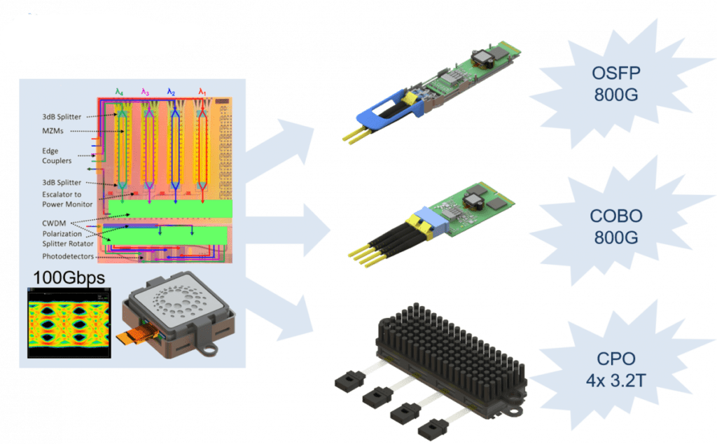
CPO Technology: Optoelectronic Integration Packaging, Significantly Reducing Power Consumption
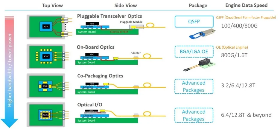
CPO technology has the advantages of low power consumption, high performance, high quality, and high transmission. With the requirements of high bandwidth computing, transmission, and storage in the 5G era, as well as the maturity of silicon photonics technology, optical interconnection has also entered the era of on-board and inter-board communication, and the number of channels has greatly increased. The packaging now requires integrating optical chips with ASIC control chips to increase interconnect density. This concept introduces the concept of optoelectronic co-packaging (CPO).
CPO refers to the optoelectronic co-packaging of the optical engine and the switching chip together. This approach allows faster transmission of electrical signals between the engine and the chip, shortening the distance between the optical engine and the switching chip, effectively reducing size, lowering power consumption, and improving efficiency.
CPO refers to the optoelectronic co-packaging of the optical engine and the switching chip together. This approach allows faster transmission of electrical signals between the engine and the chip, shortening the distance between the optical engine and the switching chip, effectively reducing size, lowering power consumption, and improving efficiency.
CPO Brings a Promising Future Market to 800G
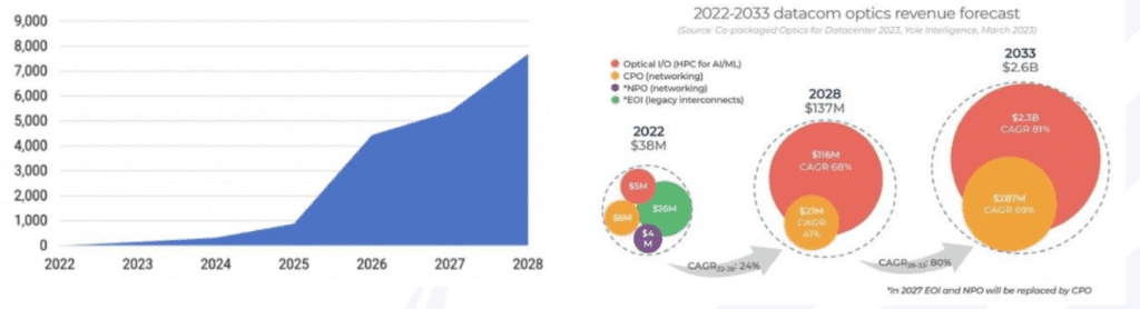
The development of CPO is currently in its early stages, with a promising future market space. CPO shipments are expected to start at 800G and 1.6T ports and enter commercial use from 2024 to 2025. By 2026 to 2027, they will scale up and primarily be applied in short-distance data communication scenarios for large-scale cloud service providers.
CPO Effectively Addresses High-speed and High-density Interconnect Transmission
The demand for network speeds driven by AI is currently more than ten times higher. In this context, CPO is expected to reduce the power consumption of existing pluggable optical transceiver architectures by 50%, effectively addressing high-speed and high-density interconnect transmission scenarios. Initially, CPO-based devices will be used in hyperscale data centers. Additionally, CPO is expected to enter other types of data centers within approximately a year and further demonstrate its advantages in areas such as edge and metropolitan networks, high-performance computing, and sensors.
The successful application of CPO technology relies on suitable material foundations, and thin film lithium niobate plays an important role in this field. As a material with excellent nonlinear optical properties, thin film lithium niobate enables optical manipulation and modulation through precise phase modulation using CPO technology. Its applications in optical modulators, optical switches, and optical waveguides provide strong support for CPO technology. By combining the characteristics of thin film lithium niobate with the flexibility of CPO technology, it offers broader possibilities for the design and manufacturing of optical devices, driving the continuous development and innovation of optical technology.
Thin Film Lithium Niobate: Significantly Smaller in Size, Facilitating High Integration
Thin film lithium niobate offers excellent performance and significant advantages in modulator fabrication schemes:
- Thin film lithium niobate exhibits multiple optoelectronic effects, including piezoelectric effect, electro-optic effect, nonlinear optical effect, optical birefringence effect, photovoltaic effect, photoelastic effect, and acousto-optic effect.
- The performance of thin film lithium niobate can be strongly controlled due to its lattice structure and abundant defect structures. Various properties of lithium niobate can be extensively regulated by crystal composition, elemental doping, and valence state control.
- Thin film lithium niobate possesses stable physical and chemical properties, making it easy to process.
- It has a wide optical transmission range, significant birefringence, and is conducive to the fabrication of high-quality optical waveguides. Therefore, optoelectronic devices based on lithium niobate, such as surface acoustic wave filters, optical modulators, phase modulators, optical isolators, and electro-optic tunable Q switches, have been widely researched and practically applied in fields such as electronics, optical communication, and laser technology.
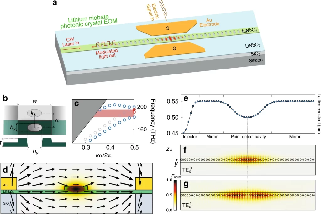
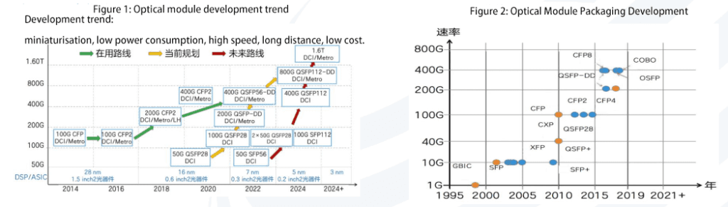
Currently, there are three fabrication schemes for electro-optic modulators. Among them, lithium niobate has significant performance advantages and can fully meet the requirements of long-distance transmission and high capacity. Depending on the materials used, these schemes can be categorized as silicon-based, phosphide-based, and lithium niobate-based. The lithium niobate-based scheme offers advantages such as high bandwidth, low insertion loss, and mature extinction ratio. Moreover, it supports transmission distances of over 100 kilometers and capacities exceeding 100G, making it widely applied in 100G/400G optical communication networks.
Comparison of Three Main Modulator Schemes
| Modulator Type | Application Scenarios | Advantages | Disadvantages |
| Silicon-based Modulator | Short-range data communication with transceiver transceivers | Small size | Average performance, not suitable for high-speed long-distance communication networks |
| Phosphide-based Modulator | Medium-range and long-range optical communication networks | High modulation efficiency, low driving voltage, adjustable bandwidth, compact device structure | High material and process requirements, high cost and integration difficulty |
| Lithium Niobate-based Modulator | Long-distance coherent communication at 100G and above | Large electro-optic coefficient, wide modulation bandwidth, low waveguide transmission loss, good stability, mature development | Relatively large size |
Although the lithium niobate scheme has performance advantages, it also has limitations:
- Performance Improvement Space: Traditional lithium niobate-based optoelectronic modulators face limitations in improving key performance parameters such as signal quality, bandwidth, and insertion loss due to the presence of free carriers in lithium niobate materials. They are also incompatible with CMOS processes.
- Size Issue: Traditional lithium niobate modulators have larger sizes, making it difficult to meet the trend of miniaturization in optical devices.
- Cost and Price Issue: The price of lithium niobate modulators is several times higher than that of indium phosphide modulators. Therefore, indium phosphide modulators have an advantage in medium-range transmission scenarios.
- Thin film lithium niobate modulators not only inherit the performance advantages of lithium niobate materials but also improve in terms of size and cost.
- Thin film lithium niobate modulators achieve new advancements in performance and cost-effectiveness, maintaining the performance advantages of lithium niobate modulators while breaking through the bandwidth limitations.
- They have significantly smaller sizes, solving the integration challenges posed by the larger volume of bulk lithium niobate materials. They enable high integration.
With the reduction in size, the unit panel transmission density is greatly increased, and there is further potential for cost reduction.
Conclusion
The combination of CPO technology and thin film lithium niobate technology brings new possibilities and opportunities to the field of optics. Their excellent performance and complementary characteristics provide powerful tools and solutions for high-speed data transmission, optical communication, artificial intelligence, and cloud computing. With ongoing research and innovation, we can anticipate the emergence of more precise and high-performance optical devices, further driving scientific and technological advancements. The coordinated synergy of CPO technology and thin film lithium niobate technology will continue to lead the development of the optical field, creating a more connected and intelligent future.