Speed, density, distance, and heat all need to be considered; pluggables still have a future.
APRIL 26TH, 2023 – BY: KAREN HEYMAN
Original from: https://semiengineering.com/new-standards-push-co-packaged-optics/
Co-packaged optics (CPOs) promise five times the bandwidth of pluggable connections, but the new architecture requires multiple changes to accommodate different applications.
The Optical Internetworking Forum (OIF) recently published standards for co-packaged optics, which are the photonic industry’s hope for handling today’s faster Ethernet interfaces, as well as increasing speeds and power requirements in the future. “800Gbs and 1.6Tbs Ethernet can utilize this technology to provide, in a power efficient way, faster Ethernet connectivity in data centers,” said Scott Durrant, strategic marketing manager at Synopsys.
The standard addresses a number of essential questions, but from a higher level of abstraction. “You have the electrical interface and the photonics interface that need to be standardized,” said Alexander Janta-Polczynski, senior advisory engineer for advanced semiconductor packaging at IBM, an OIF member who participated in the committee. “What kind of connectors are you going to use? How are you going to build the interface? How are you going to test it? What kind of electrical speeds will you be wiring? There’s not one single standard that came out because the various applications have some specific challenges. It’s more of a template of what is required for CPO, but it’s very useful.”
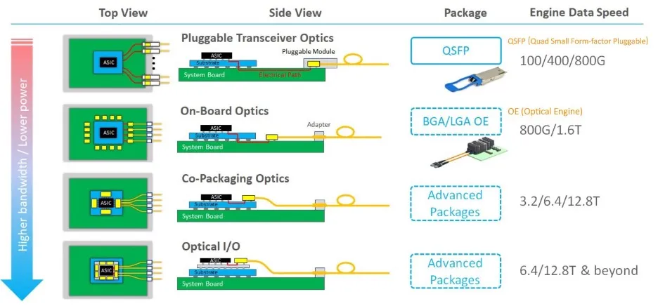
CPO is a rethinking of architecture to minimize latency and reduce energy use. The solution is similar to near-compute strategies in CMOS layouts — efficiencies are achieved by placing basic elements that need to communicate closer together. In photonics, the standard configuration was a switch chip with electrical traces that ran all the way across the board to the front panel, where pluggable optics were inserted.
That worked well for three decades, but as data rates increased, the energy inefficiencies became more obvious. “Front pluggables are very hard on power usage,” said Janta-Polczynski. “Because the system needs to send electrical signals, they need repeaters — SerDes that serialize the data and send it through the PC up to the front panel. This consumes a lot of energy. When you’re reaching those big switch speeds in AI applications that are really data-hungry, the power consumption is extremely intense and detrimental.”
Others agree. “The amount of energy required to move data from the switch chip — the ASIC — to the optical module on the front panel of the switch is becoming untenable, at about 8 picojoules per bit,” said Durrant. “A switch that is carrying 400 gigabits Ethernet equates to about 100 watts of power within this chip to move data between this switch ASIC and the pluggable module at the front panel. That’s manageable, but as switches increase in speed, the amount of energy required is going to grow to 200 or 400 watts. And that becomes something that’s very difficult to cool.”
At that point, engineers started considering a scheme called “on-board optics,” with the idea of making optical modules a little smaller and putting them closer to the ASIC. Unfortunately, it didn’t quite work. Once all the desired capabilities were incorporated into the standard, the optical modules ironically came out larger than before and the power savings weren’t achieved.
That lesson learned, the latest approach is called “co-packaged optics,” in which the optical module is moved onto the same substrate as the switch ASIC. This allows data to move a very short distance on a very low-loss substrate. And with the expectation that the energy required will be much less than three picojoules per bit, it should be possible to move data at 1.6 terabits per second or faster.


Fig. 1: Evolving toward co-packaged optics. Source: Synopsys
“There is a lot of work on co-packaged optics,” according to Robert Maher, CTO for optical modules and coherent solutions at Infinera. “Vendors such as Broadcom and Intel are developing co-packaged optics that can be replaced through a plug-and-play assembly. All co-packaged optics are highly parallelized and integrated inside the switch router. They are typically implemented in SiPh with a pluggable-based laser, which is also plugged into the switch faceplate. The goal here is to replace low-reach pluggables inside the data center. The switch router with co-packaged optics will have optical I/O at the faceplate.”
The recently announced standard from the OIF defines a 3.2T co-packaged module that targets Ethernet switching applications. It utilizes 100G electrical lanes and provides backward compatibility with 50G lanes. Further, the module definition can be in the form of an optical module or a passive copper cable assembly, providing about 140G/mm of bandwidth edge density. It can enable optical and/or electrical interfaces for a 51.2Tb/s aggregate bandwidth switch.
This approach also solved a more basic problem — optical components are highly sensitive to temperature, which can cause failures. And given the complexity of the assembly, that can decrease manufacturing yield. That made it imperative to allow replacements during assembly.
“It was agreed to do a socket approach for a co-packaged assembly,” said Jeff Hutchins, who serves as a board member and vice chair of the PLL Working Group for Co-Packaging at OIF, as well as director of the CTO office at Ranovus. “Co-packaging can drop the power level, because you’re now transmitting on electrical traces that are right on the substrate and not very long.”
To go into more detail, the new implementation agreement includes interoperability specifications for the 3.2 Tb/s CPO modules including an 8x400Gb/s optical interface connectivity option for FR4 (four optical channels on one fiber) and DR4 (one fiber per channel, with four different fibers).
“FR4 and DR4 are standards that have been around for years. Usually, they’re given names like 400GBASE-DR4, which means it’s a 400G link. As the data rates go up, the acronyms stay around, it just means there’s four lanes per fiber even as the data rate increases,” explained Hutchins. “The 3.2 T module has eight of those interfaces in one module so each fiber carries one lane per fiber (DR) or four 100 G lanes per fiber (FR). That makes it a 400G interface, and we’ve packed eight of those into one module.”
To understand the scale difference, consider that a pluggable module is usually in the range of 18mm wide by 80mm long, and has just one 400G link, while the new standard describes a module that can contain eight. “It’s much higher density than what people are used to in a much smaller form factor,” said Hutchins.
The standard also specifies a 32 x CEI-112G-XSR (extra short reach) host interface (or 32 x CEI-56G-XSR in “backwards compatible” mode).
“In a regular Ethernet switch, rack or shelf, they would use a very short reach interface to get to the front panel,” Hutchins said. “This is an extra short reach, which means it’s a lot lower power, something less than 2 picojoules per bit. It only can reach about 50mm, which makes it perfect for an on-substrate connection between the ASIC chip and this optical engine. The specification was for 112G, but it essentially carries 100G of data along with the necessary overhead.”
One of the main value propositions of co-packaging is to reduce the overall power consumption, but there is a challenging flipside — power density. “In a regular switch card, you have all the pluggable modules at the front panel getting cooled with incoming air,” he said. “And then you have the switch chip in the back, with fans other solutions it to cool it down. But while CPO reduces the overall power consumption, the power density is very high in that CPO packaged area, because you just put a lot more stuff there than you had before. Because of the power density, the thermal management is a lot more complicated. It may have to be re-thought in some applications.”


Fig. 2: Evolving optics layouts — a slightly different view. Source: ASE
The Future: How soon is now?
There is even a potential alternative to co-packaged optics, in the form of linear drive optics, which was first presented last October by NVIDIA. As described by OIF in its post-show report, there are similarities with CPO. “In both cases, one of the two DSPs is removed from the link, reducing power consumption. CPO moves the optics closer to the ASIC, but linear-drive pluggable optics remain at the front panel of the switch.”
Various forms of pluggables may continue to be state-of-the-art for a surprisingly long time. “Last year at OFC, there was a ton of talk about co-packaged optics,” said Rob Shore, senior vice president of marketing, Infinera. “You would have expected a significant amount of progress given all that talk, but it was almost the exact opposite. Most people were saying, ‘Hey, we made so much progress on pluggable optics, bringing down the cost and enabling higher capacity, that it looks like it’s probably pushed out the drive for co-packaged optics by a couple of years at least.”
Part of that is driven by a host of challenges, said Infinera’s Maher. “Challenges revolve around vendor lock-in, switch plus optics supplied by a single vendor, such as BRCM. Hyperscalers typically have a large amount of control over the vendors of their intra-DC pluggables. Meta and Google stated at OFC that they would stick with pluggables for the 50T class of switch routers. Another challenge is the failure aspect of the co-packaged optics part. Each SiPh part carries 6.4T in a BRCM Tomohawk 5 box. If one lane goes down, you need to take the box out, open it up and replace the entire 6.4T receptacle. Current approach, if you have a bad plug, you bin it and replace with another one.”
And then there’s the practical aspect: “I was walking around OFC and asking the people making these optics, are you shipping these?” said Michael Klempa, OIF interoperability chair. “And they said, no. I think they built a solution to a problem that doesn’t need to be solved immediately. But everyone agrees it’s going to need to be solved eventually. So it’s good that people are putting in the work right now.”
Or as, IBM’s Janta-Polczynski declared, “A standard for CPO is essential for photonics’s emergence as a disruptive technology.”
Finally, regarding the debate between CPO and pluggables, Michael Lebby, CEO of Lightwave Logic, observed that the standards include both an internal laser source as well as an external laser source. “An external laser source is a pluggable module,” he said. “I thought the whole concept of co-packaged optics was to get rid of the pluggable module. But now they’re bringing it back, which means there is a group that believes external laser driving is the right way to go — maybe because of reliability, maybe because you’ve got one big powerful laser as opposed to a lot of onboard lasers that could be subject to reliability and heat issues. So what’s the right form factor? If the co-packaged optical module that gets really close to the electrical switch chip is small enough that it could fit into a pluggable form factor, as well, whoever makes those modules gets a double win.”
Related Content
Co Packaged Optics In The Data Center (Semiconductor Engineering video).https://www.youtube.com/watch?v=lC0i7_ilpf8&ab_channel=SemiconductorEngineering
Will Co-Packaged Optics Replace Pluggables?
New options open the door to much faster and more reliable systems.

